波長ドメイン光スイッチ
1.研究背景
次世代の光ネットワークでは、
•混雑回線の回避
•障害(断線など)回避
といった観点から、信号経路の最適化が波長成分別に行われ、信号経路は時々刻々と変化する。
⇒ノードを構成する光スイッチが不可欠
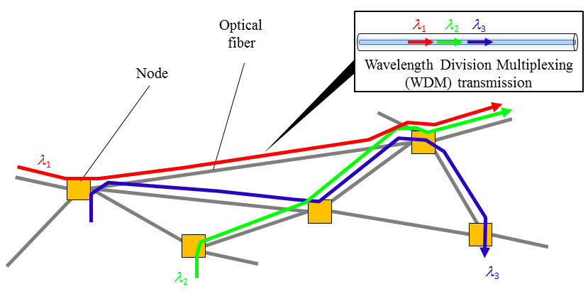
Fig.1 Wavelength routing on WDM networks
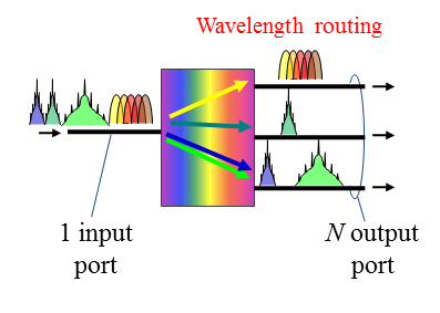
Fig.2 Wavelenth selective swicth
研究目的
自由空間型の大規模波長選択スイッチ(WSS)について、高機能化を検討。
2.LCOS型WSS
研究項目1
従来のLCOS型 WSSはバルク光学部品を必要とするため、構成が複雑化。
⇒大型化・組み立てコスト増大・信頼性低下
分光光学系として多層アレイ導波路回折格子(AWG)を用いる
⇒バルク回折格子とビーム整形光学系が不要下
⇒構成簡素化
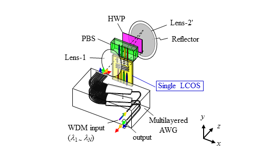
Fig.3 LCOSS-WSS using multi-layed AWG with polarization compensation
研究項目2
AWGの位相誤差(導波路層・偏波モードによる)が障壁となり、実用的なWSSを得ることが難しい
⇒損失・PDLの悪化
LCOSで位相変調を行うことで位相誤差補償を行う
⇒低損失化・低PDL化
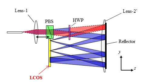
Fig.4 Swicthing operation of proposed WSS
研究項目3
LCOSが高コスト
•AWGの位相誤差補償動作
•スイッチング動作
の両方を、1台のLCOSで行うことが可能なWSSの構成法を提案
⇒低コスト化・小型化
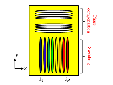
Fig.5 Image layout on LCOS
スイッチング特性
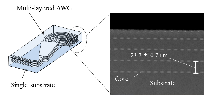
Fig.6 Multi-arrayed AWG
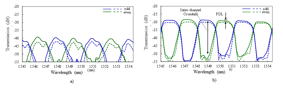
Fig.7 Transmission spectrum of WSS showing switching operation a) Without polarization error compensation b) Polarization error compensated
40Gbit/s信号伝送実験結果
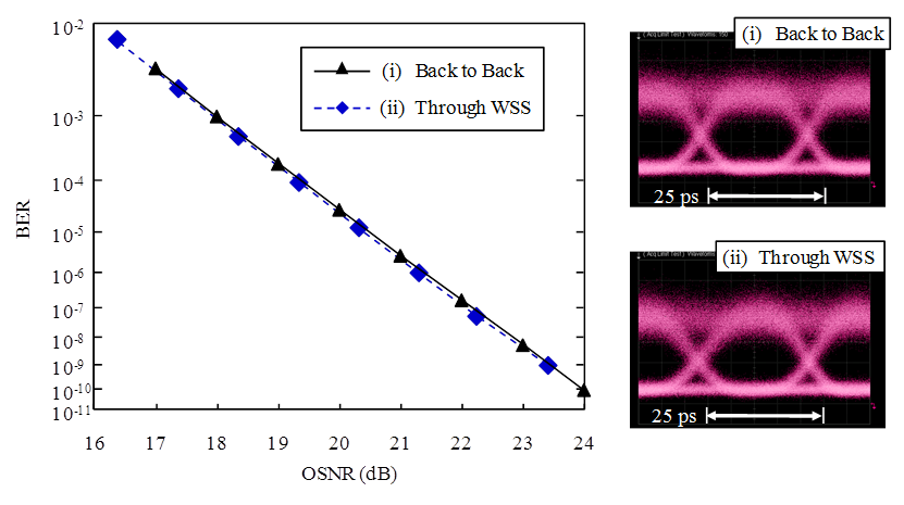
Fig.8 40Gbps signa; transmission experiment
3.MEMS型WSS
研究項目4
MEMSを用いたWSSにおいて可変グリッド動作時、スペクトルリップルが発生案
⇒低コスト化・小型化
ミラー表面にスロット構造を設けることで、反射損失を均一化
⇒リップル抑圧
⇒可変グリッド動作が可能となる
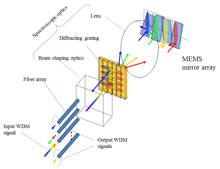
Fig.9 MEMS-WSS
スペクトル計算
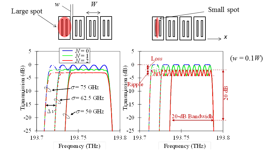
Fig.10 Transmission spectrum calculation in the case of a) large spot size and b) small spot size. N is the number of slot on a mirror
4.本研究に関する研究発表リスト
| (a).論文 | |
|---|---|
| [1] |
Keisuke Sorimoto, Ken Tanizawa, Hisato Uetsuka, Hitoshi Kawashima, Masahiko Mori, Toshifumi Hasama, Hiroshi Ishikawa, and Hiroyuki Tsuda
“Compact and Phase-Error-Robust Multilayered AWG-based Wavelength Selective Switch Driven by a Single LCOS,”
Optics Express Vol. 21, Iss. 14, pp. 17131-17149 (2013).
|
| [2] |
Keisuke Sorimoto, Hitoshi Kawashima, Masahiko Mori, Toshifumi Hasama, Hiroshi Ishikawa, Hiroyuki Tsuda, and Hisato Uetsuka,
“MEMS mirror with slot structures suitable for flexible-grid WSS,”
IEICE Electron. Express, Vol. 10, No. 3, pp. 20120924 (2013). DOI: 10.1587/elex.10.20120924.
|
| [3] |
K. Sorimoto, K. Kintaka, H. Kawashima, M. Mori, T. Hasama, H. Ishikawa, H. Tsuda, and H. Uetsuka,
“Phase Error Compensation for Multilayered AWG in LCOS-based WSS,”
IEICE Electron. Express, Vol. 8, No. 24, pp.2054-2060, Dec. 25 (2011).
|
| [4] |
K. Sorimoto, K. Kintaka, H. Kawashima, M. Mori, T. Hasama, H. Ishikawa, H. Tsuda, and H. Uetsuka,
“Fast Aberration-Correcting Algorithm for an SLM-based Optical Switch,”
IEICE Electron. Express Vol. 7, No. 23, pp. 1728-1734(2010).
|
| (b).国際会議発表 | |
|---|---|
| [5] | K. Sorimoto, K. Kintaka, H. Kawashima, M. Mori, T. Hasama, H. Ishikawa, H. Tsuda, and H. Uetsuka, “1×6 Multicasting Operation in an LCOS-and-AWG-based Wavelength Selective Switch,” 1st International Symposium on Access Spaces (IEEE-ISAS 2011), GS3-B-3, Yokohama, Japan, Jun. 18 (2011). |
| [6] | K. Sorimoto, H. Tsuda, H. Ishikawa, T. Hasama, H. Kawashima, K. Kintaka, M. Mori, and H. Uetsuka “Polarization Insensitive Wavelength Selective Switch Using LCOSs and Monolithically Integrated Multi-layered AWG,” 15th Optoelectronics and Communications Conference (OECC 2010),6E2-4, July 5-9, Sapporo, Japan (2010). |
| [7] | K. Sorimoto, H. Tsuda, H. Ishikawa, T. Hasama, H. Kawashima, K. Kintaka, M. Mori, and H. Uetsuka, “Demonstration of a Wavelength Selective Switch Using an LCOS and a Stacked Arrayed Waveguide Grating,” 35th European Conference and Exhibition on Optical Communication (ECOC) 2009, P. 2.04, Sep. 20-24, Vienna, Austria, (2009). |
| [8] | K. Sorimoto, H. Tsuda, H. Ishikawa, T. Hasama, H. Kawashima, K. Kintaka, M. Mori, H. Uetsuka, “Design of a wavelength selective switch using an LCOS and a multi-stacked AWG fabricated on wedge-shaped substrates,” International Topical Meeting on Information Photonics (IP2008), 3-P4, Nov. 16-20, Hyogo, Japan (2008). |
| [9] | K. Sorimoto, H. Tsuda, H. Ishikawa, T. Hasama, H. Kawashima, K. Kintaka, M. Mori, H. Uetsuka, “A Compact High-Port-Count Wavelength Selective Switch Using LCOSs and a Multi-Stacked AWG,” The 21st Annual Meeting of the IEEE Lasers & Electro-Optics Society 2008, TuCC2, Nov. 11, Newport Beach, USA, (2008). |